The Auger effect reveals intriguing details about atomic interactions. Discovered by French physicist Pierre Auger in 1923, this phenomenon provides key insights into how atoms behave after being excited. Understanding the Auger effect is essential for applications in various fields, from materials science to semiconductor technology.
What is the Auger Effect?
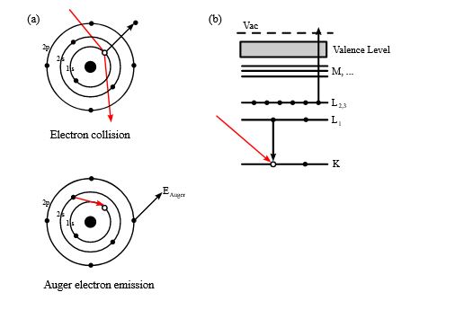
The Auger effect occurs when an atom releases an electron after losing an inner-shell electron. Here’s a simple breakdown of the process:
- Initial Ionization: An inner-shell electron is knocked out of the atom by an X-ray photon or another high-energy particle. This creates a vacancy in the inner shell.
- Energy Release: An electron from a higher energy level falls into the vacancy. Instead of emitting X-rays, the atom uses this energy to eject a second electron.
- Auger Electron Emission: The ejected electron, known as an Auger electron, carries away the energy from the transition.
Key Characteristics
- Energy Levels: The energy of the Auger electron is specific to the difference between the two electron shells involved in the transition.
- Analytical Tool: Auger electron spectroscopy (AES) uses the Auger effect to analyze the surface composition of materials. This method provides detailed information about the elements present.
- Element-Specific: The Auger effect is useful for determining the presence and concentration of elements, making it a powerful tool for surface analysis.
Applications of the Auger Effect
1. Surface Analysis
In materials science, Auger electron spectroscopy (AES) is used to examine the surface composition of various materials, including metals and semiconductors. By analyzing the emitted Auger electrons, scientists can identify the elements on a material’s surface and their concentrations.
2. Semiconductor Research
The Auger effect is crucial for studying semiconductor materials. Researchers use AES to evaluate the quality and composition of semiconductor surfaces, which is essential for developing electronic devices.
3. Thin Film Analysis
AES helps in analyzing thin films and coatings. It provides information about the elemental distribution and thickness, which is important for applications in coating technology and nanomaterials.
Historical Context
Pierre Auger’s discovery of the Auger effect was a milestone in atomic physics. Initially a scientific curiosity, the Auger effect has become an essential tool in many scientific and industrial applications. Advances in spectroscopy and imaging technology have further enhanced its significance in material analysis.
The Auger effect is a vital phenomenon in atomic physics, offering valuable insights into atomic interactions and material surfaces. Its applications in surface analysis, semiconductor research, and thin film evaluation highlight its importance in modern science and technology. By understanding the Auger effect, scientists and engineers can better analyze and develop new materials and technologies.